The AI economy is discovering that intelligence is not priced by the processor alone, but by the memory that can feed it fast enough.
The sticker shock starts at the shelf
In late 2025, RAM stopped behaving like a commodity. In Tokyo’s Akihabara district, shops removed fixed price tags from memory modules and began quoting spot prices on whiteboards. In North America, Micro Center moved RAM to dynamic pricing. A 32-gigabyte DDR5 kit that cost around $120 in May was selling for $410 by December, a 242 percent increase in seven months. [1] [2]
The underlying chip moved even faster. A 16-gigabit DDR5 chip averaged $6.84 in September 2025. By November 19, it traded at $24.83, then reached $27.20 in December. [1] Framework began charging $10 per gigabyte for DDR5 upgrades and publicly explained the change. [3] By the first quarter of 2026, TrendForce said conventional DRAM prices had risen 93 to 98 percent quarter-over-quarter, while PC memory rose by more than 100 percent in a single quarter. [4] [5]
The tiny leaking bargain
DRAM became cheap because Robert Dennard’s 1966 idea reduced memory to a brutally elegant cell: one transistor and one capacitor. The transistor opens and closes the gate. The capacitor holds charge. Charged means one; empty means zero. Reading the bit lets charge flow onto a bit line, where a sense amplifier detects the voltage. Writing drives charge in or out. [6] [7] [8]
The genius was also the flaw. Capacitors leak. Every DRAM row must be refreshed before its charge fades, and JEDEC specifies refresh every 64 milliseconds. [6] That means billions of cells are constantly being read and rewritten even when no software asks for data. As cells shrink, the storage capacitor becomes an extreme structure, with aspect ratios approaching 100:1, and a tiny impurity can ruin yield. [9] [10] Modern 3D DRAM manufacturing can exceed 1,000 process steps over 12 to 16 weeks. [11] [12] Cheap memory was never simple. It was simply mastered at scale.
The three survivors
The current crisis is harder to solve because the DRAM industry has been consolidated by half a century of price wars, industrial policy, recessions, and bankruptcies. American firms dominated early DRAM. Japan overtook them by the 1980s, reaching roughly 80 percent of global DRAM sales by 1987. [13] [14] Washington responded with the 1986 U.S.-Japan Semiconductor Trade Agreement, then 100 percent punitive tariffs in 1987, while DARPA helped create SEMATECH to rebuild U.S. competitiveness. [15] [16] [17]
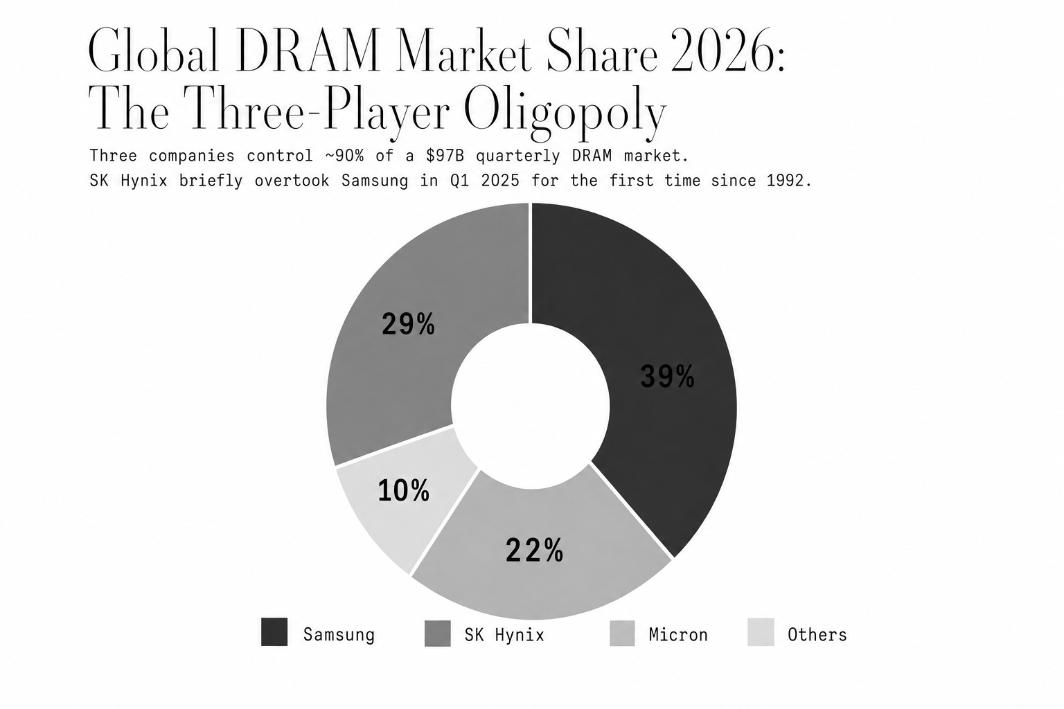
Then South Korea rose. Samsung commercialized major DRAM generations, while Hynix survived a government-orchestrated rescue after the Asian financial crisis. The U.S. Commerce Department later treated Hynix’s restructuring as actionable subsidies and imposed a 57.37 percent countervailing duty in 2003. [18] Japan’s last DRAM champion, Elpida, filed for bankruptcy in 2012 and was acquired by Micron. [19] The result is today’s market: Samsung, SK Hynix, and Micron together control approximately 90 percent of DRAM revenue. [20]
Why AI eats memory first
A large language model is, physically, an enormous set of numbers that must be kept close to compute. A 70-billion-parameter model using 16-bit values needs 140 gigabytes just for weights before it generates a token. [21] During inference, the system also stores a key-value cache of prior tokens. With a 128,000-token context window and optimization, that cache can consume roughly 40 gigabytes. Without such techniques, OPT-175B can require approximately 950 gigabytes of cache for certain batched workloads. [22]
Training is worse. Adam, a standard optimizer, stores two additional momentum buffers per parameter. A 70-billion-parameter model in mixed-precision training needs roughly 840 gigabytes for persistent training state before activations, gradients, or batch data. [23] The limiting factor is often not arithmetic. It is movement. Research found DRAM bandwidth saturation accounted for more than 50 percent of attention kernel cycles stalling on data access delays. [24] In AI, memory is not storage. It is the road system.
Demand has gone parabolic.
HBM turns the road into a vertical city
High-Bandwidth Memory is the industry’s answer to the bandwidth wall. Instead of placing memory chips on a module across a circuit board, HBM stacks DRAM dies vertically and drills microscopic copper columns through the silicon, called through-silicon vias. SK Hynix produced the first HBM chip in 2013, and JEDEC standardized the category that year. [25] [26]
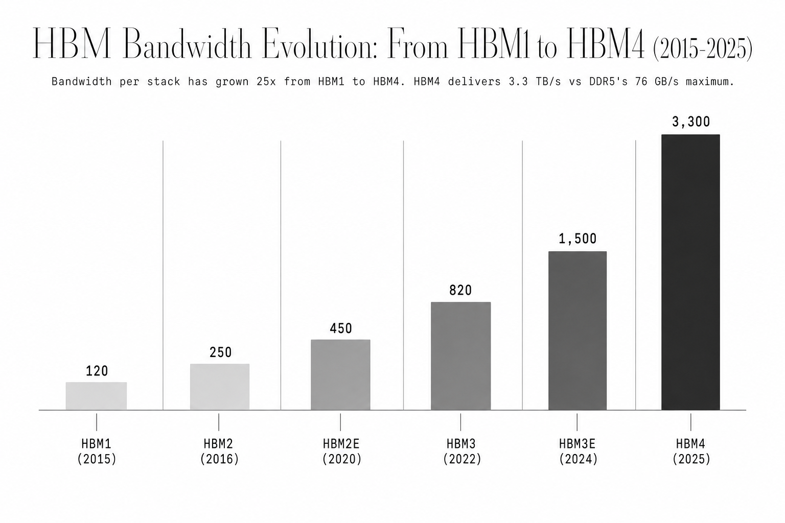
The payoff is width. A single HBM3 stack has a 1,024-bit interface, compared with 64 bits for a standard DDR5 DIMM. Six HBM3 stacks on NVIDIA’s H100 deliver 3.35 terabytes per second of bandwidth. [27] The H200 raises that to 141 gigabytes of HBM3e and 4.8 terabytes per second. [28] NVIDIA’s Vera Rubin platform is designed around eight HBM4 stacks, 288 gigabytes of capacity, and 22 terabytes per second per GPU. [29] [30]
But the architecture is expensive because it is unforgiving. HBM yields can run 55 to 75 percent, versus 85 to 95 percent for conventional DRAM. [31] A single defective die can ruin a stack.
The raw materials are not raw at all
The memory supply chain begins with geology, but it is governed by purity. Silicon wafers require nine-nines purity, and advanced applications can require 11 or 12 nines. Wacker Chemie produces 12-nines polysilicon, meaning no more than one foreign atom per trillion silicon atoms. [32]
Other dependencies are narrower. Before Russia’s 2022 invasion, Ukraine produced between 40 and 70 percent of global semiconductor-grade neon, and the United States sourced as much as 90 percent of its supply from Ukrainian producers. [33] [34] Hafnium, used in modern high-k dielectrics, exists mainly as a byproduct of nuclear-grade zirconium production. Global output runs at about 75 metric tons per year, while projected semiconductor demand was reaching 150 to 200 metric tons by 2025. [35] Copper reached an all-time high above $11,600 per metric ton in December 2025. [36] Yttrium prices rose from about $8 per kilogram to $126 per kilogram through 2025 after Chinese export controls tightened. [37] Memory is sand, but only after the planet has been refined.
The factory cannot hurry
The standard cure for a shortage is capacity. In DRAM, capacity is a five-year decision. A leading-edge memory fab costs roughly $14 billion to $36 billion. Samsung’s P4 fab in Pyeongtaek is estimated at about $36 billion, and SK Hynix’s M15X in Cheongju at roughly $14 billion. [38] A large fab can require 30 to 40 million workhours, 83,000 tons of steel reinforcement, 5,600 miles of cabling, and 785,000 cubic yards of concrete. [39]
The key equipment is even more constrained. ASML is the sole supplier of extreme ultraviolet lithography systems used for the finest semiconductor features. A Low-NA EUV system costs roughly $150 million to $170 million; High-NA systems cost around $380 million. [40] Each machine ships in 250 crates, needs more than three cargo aircraft, and takes six months and 250 specialized engineers to assemble. [40] As of 2025, 51 percent of EUV shipments were configured for memory production. [41] Capital can be approved overnight. Yield cannot.
Policy can subsidize, but not teleport
Washington has returned to chips with money and denial. The CHIPS and Science Act provides $52.7 billion in total, including $39 billion for manufacturing incentives and a 25 percent advanced manufacturing investment tax credit. [42] [43] Micron received $6.165 billion for facilities in New York, Idaho, and Virginia; Samsung received $4.745 billion for its Taylor, Texas complex; SK Hynix received $458 million plus up to $500 million in loans for an HBM packaging facility in Indiana. [44] [45] [46]
The SK Hynix project shows the limit. Its $3.87 billion Indiana facility will package HBM, not fabricate wafers. It will receive pre-built, tested HBM stacks from Korean fabs and assemble finished products. [47] [48] Meanwhile, export controls seek to deny China the equipment and GPUs needed for advanced chipmaking. The October 2022 BIS rules restricted equipment for chips below 16 nanometers and blocked advanced NVIDIA GPUs from China, with later rules tightening the system further. [49] [50] Policy can reshape geography. It cannot compress semiconductor time.
Until further notice
The memory shortage is not a one-off squeeze. It is a structural collision between an industry that changes over years and an AI demand curve that changed over months. Samsung, SK Hynix, and Micron have announced more than $50 billion in new HBM investments. [2] [51] Micron raised 2026 capex to $20 billion and announced a $24 billion Singapore investment; Samsung is increasing HBM capacity by about 50 percent in 2026. [52] [53] Those projects matter, but meaningful relief is unlikely before 2027 or 2028 because fabs cannot skip construction, qualification, and yield ramps. [54]
Each accelerator generation also consumes more HBM than the last: 80 gigabytes in H100, 141 gigabytes in H200, and 288 gigabytes planned for Vera Rubin. [29] Industry leaders have pointed to relief only in 2028 or later, with SK Group’s chairman estimating the shortage could persist until 2030. [52] [55] The price of AI is increasingly the price of memory, and memory is increasingly the slowest thing in the system to make more of.
- DRAM became cheap through a deceptively simple one-transistor, one-capacitor cell, but that cell leaks and requires extreme manufacturing precision at modern scale.
- AI workloads are memory-bound: the expensive part is not only computing numbers, but moving vast model weights and caches quickly enough to keep GPUs busy.
- HBM solves the bandwidth problem by stacking memory vertically, but its yields, packaging complexity, and per-gigabyte costs make it structurally expensive.
- New subsidies and fabs will help, but the supply response is measured in years, while AI demand has been repriced in months.
Get the next issue in your inbox.
Free, weekly. One company or market, taken completely apart — every figure sourced and verified with Valyu DeepResearch.
Issue queued.
Your next cited briefing is on its way to .