There is a building in Veldhoven, a small Dutch city best known for being adjacent to Eindhoven, where engineers assemble the most complex machines ever manufactured.
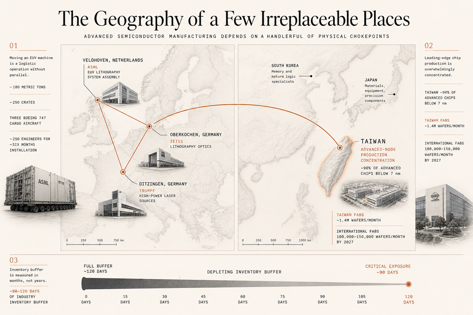
The building is unassuming. The machines are not. Each one weighs roughly 180 metric tons, travels to its destination in 250 shipping crates aboard three Boeing 747 cargo aircraft, and requires 250 engineers approximately six months to install and calibrate after arrival. Each one costs, depending on the model, somewhere between $150 million and $400 million. And each one is built by a single company in the world, a Dutch firm called ASML, which has no meaningful competitor and without which the production of virtually every advanced semiconductor on Earth would halt within months. [1] [2] [3]
The iPhone in a pocket, the Nvidia chip accelerating a language model, the processor managing braking in a modern car, the memory in a data center running cloud services for hundreds of millions of people: all of these trace their existence, somewhere upstream in their manufacturing chain, to one of the machines assembled in Veldhoven. This is not an exaggeration. It is a structural fact about how the modern world produces the components it now depends upon absolutely.
The Problem of Light
To understand why ASML exists and why no one else can do what it does, the story has to begin with physics.
Making a semiconductor chip is, at its core, an act of printing. A pattern representing billions of transistors is projected onto a silicon wafer coated with a light-sensitive chemical. Where the light strikes, the chemistry changes. The exposed material is then etched away or retained, layer by layer, until a working circuit emerges from what was once blank silicon. The technique is called photolithography, and the machine that performs it is called a lithography scanner.
The resolution of any optical system, meaning the smallest feature it can print, depends on the wavelength of the light it uses. The relationship is captured in the Rayleigh criterion: critical dimension equals a process constant multiplied by wavelength, divided by numerical aperture. Shorter wavelengths print smaller features. For decades, the semiconductor industry pushed light sources toward shorter and shorter wavelengths. Lamps gave way to ultraviolet lasers. By the early 2000s, the dominant technology used argon fluoride lasers at 193 nanometers, roughly one five-hundredth of the width of a human hair. Chipmakers squeezed extraordinary mileage from this wavelength using a technique called immersion lithography, which places a thin film of purified water between the final lens element and the wafer, effectively increasing resolution by changing how light bends. They then extended it further with multi-patterning: instead of printing a feature in one exposure, they would decompose the pattern into multiple simpler passes, each slightly offset from the last. [4]
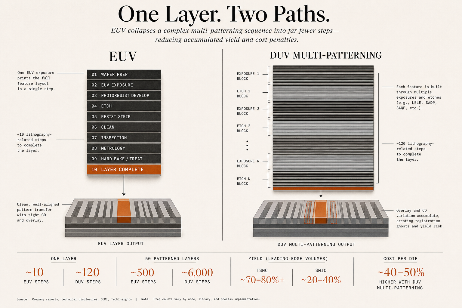
The cost of this extension was steep. At the 5-nanometer node, a single layer that a modern extreme ultraviolet machine handles in a single exposure requiring roughly 10 process steps demands, with the older deep ultraviolet approach and its most advanced multi-patterning variant, approximately 120 steps. Across the 50 or so patterned layers in an advanced chip, that compounds: an extreme ultraviolet process requires around 500 total lithography-related steps, while a deep ultraviolet multi-patterning equivalent requires around 6,000. The yield penalties and cost premiums are severe. China's SMIC, which manufactures advanced chips without extreme ultraviolet access, achieves yields of roughly 20 to 40 percent on its most advanced processes, compared to 70 to 80 percent or more at TSMC using extreme ultraviolet, and its cost per die runs approximately 40 to 50 percent higher. [4] [5] [6]
The industry needed a fundamentally shorter wavelength. What it found, after decades of research, was extreme ultraviolet light at 13.5 nanometers, roughly 14.7 times shorter than the 193-nanometer light used in deep ultraviolet systems. The physics of this wavelength presented an immediate problem: at 13.5 nanometers, light is absorbed by virtually everything, including air, glass, and all conventional optical materials. Every component of a conventional lithography machine, the lenses, the environment through which the beam traveled, the gas in the chamber, would simply swallow the light before it reached the wafer. [7] [8]
Building a machine that works at this wavelength required abandoning almost every assumption that had governed optical lithography for half a century.
How the Light Is Made
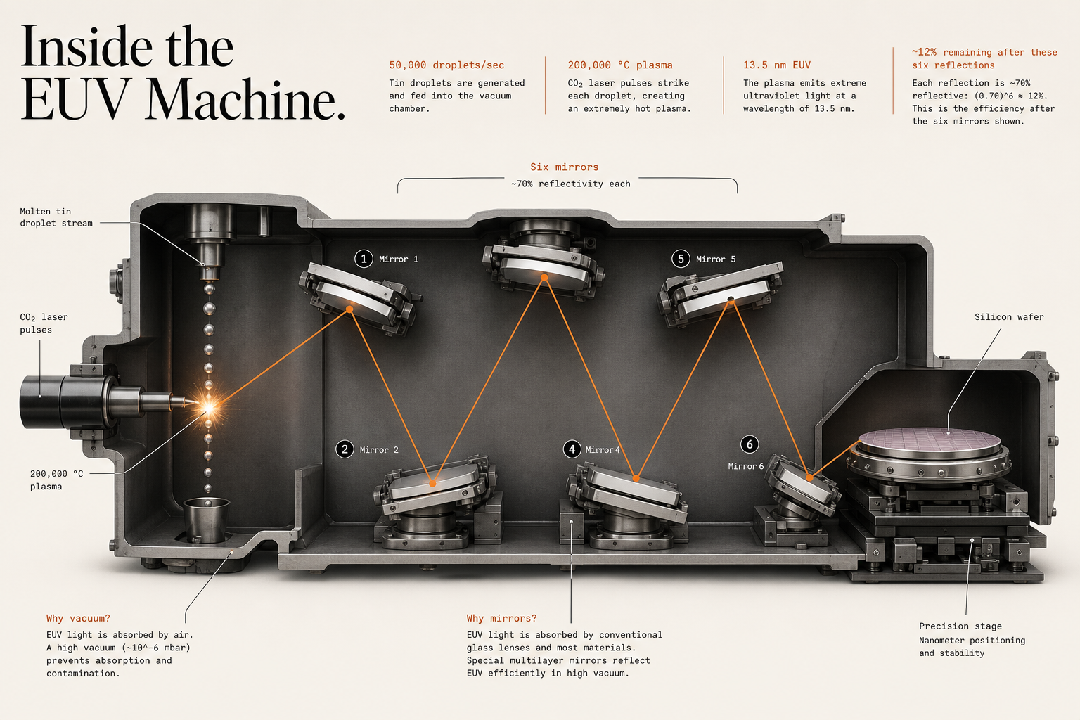
ASML's extreme ultraviolet lithography machines generate light through a process that reads more like alchemy than engineering. A generator fires molten tin droplets through a vacuum chamber at a rate of around 50,000 per second. A high-powered carbon dioxide laser produced by the German company Trumpf, two of which are required per machine, strikes each droplet and vaporizes it into a plasma heated to approximately 200,000 degrees Celsius, around 40 times hotter than the surface of the sun. This plasma, composed of multiply ionized tin atoms in charge states ranging from Sn8+ to Sn14+, radiates at 13.5 nanometers. [9] [10] [11]
The choice of tin is not incidental. It is the only element that emits strongly enough at 13.5 nanometers to be commercially viable, and it does so because that wavelength coincides precisely with the peak reflectivity of the mirrors that must collect and direct the light. Those mirrors, manufactured exclusively by Carl Zeiss's semiconductor division in Oberkochen, Germany, are built from 50 alternating layers of molybdenum and silicon, each bilayer roughly 7 nanometers thick. The layers interact via Bragg reflection, a physical phenomenon in which precisely spaced thin films cause light waves to reinforce each other constructively at a specific wavelength and angle. At 13.5 nanometers and normal incidence, each mirror reflects approximately 70 percent of incoming light. [12] [13] [14]
The surface of each mirror must be polished to a deviation of 50 picometers root mean square, 50 trillionths of a meter. Zeiss illustrates the scale of this requirement with an analogy: if a finished EUV mirror were enlarged to the size of Germany, the tallest imperfection on its surface would stand roughly one millimeter high. [15] [2]
Because six such mirrors form the projection system in a standard machine, and because each reflects only about 70 percent of the light that strikes it, the chain of reflections reduces the original source power dramatically. After six mirrors, roughly 12 percent of the initial photon flux reaches the wafer. The source, therefore, must be extraordinarily powerful. ASML achieved 250 watts of sustained EUV output in 2018, enabling throughput of 125 wafers per hour. In April 2025, the company demonstrated 1,000 watts under production-realistic conditions, a milestone that took the light source program from a single watt in 2010 through a sequence of decade-spanning engineering achievements to reach. The current third-generation scanner, the NXE:3800E, achieves a record throughput of approximately 230 wafers per hour. [16] [17] [18]
The entire optical path operates in high vacuum. There is no other option at this wavelength. Even trace concentrations of gas would absorb the beam before it completed its journey from source to wafer. A standard extreme ultraviolet illumination system contains approximately 15,000 individual parts and weighs 1.5 metric tons. The projection optics add roughly 20,000 parts and another 2 metric tons. [19] The full machine, integrating the light source, optics, wafer stage, reticle handler, vacuum systems, control electronics, and software, represents over 100,000 components sourced from more than 800 suppliers across three continents. [11] [20]
Three Decades of Improbable Engineering
ASML's path to this machine was neither inevitable nor smooth. The company was founded in 1984 as a joint venture between Philips and the Dutch-listed firm ASM International, operating initially out of a leaky shed adjacent to Philips buildings in Eindhoven. By 1988, with the global semiconductor industry in a cyclical trough, ASM sold its stake back to Philips, which now owned the struggling venture entirely. Internal accounts describe the period as one of near-bankruptcy. Frits van Hout, later ASML's Chief Strategy Officer, recalled that colleagues at the time were asking one another whether they were there voluntarily. [21] [22]
Survival came through engineering execution rather than financial rescue. ASML's 1991 machine, the PAS 5500, used optics supplied by Carl Zeiss under an agreement that dated to 1983, and its modular, serviceable design impressed IBM's director of semiconductor research enough that IBM became the company's first major customer. The machine's ability to be repaired quickly on-site, with parts easily replaced, gave it an operational advantage over the more vertically integrated systems of Japanese competitors Nikon and Canon, which at that point controlled roughly 75 percent of the global lithography market. [23] [24]
The critical strategic bet came in 1997. Japan's Hiroo Kinoshita at NTT had demonstrated the first-ever EUV lithographic images in 1986, adapting multilayer mirror research that had originated in Soviet x-ray optics work. American researchers at Lawrence Livermore National Laboratory followed through the late 1980s. In March 1997, a consortium led by Intel, with co-founders AMD and Motorola, signed a Cooperative Research and Development Agreement with three Department of Energy national laboratories: Lawrence Livermore, Sandia, and Lawrence Berkeley. This became the Extreme Ultraviolet Limited Liability Company, the largest such public-private partnership in DOE history at the time, committing $250 million over the initial three-year term. [25] [26] [27]
The consortium's structure determined the competitive landscape for the next three decades. Nikon and Canon were excluded, on Cold War-era national security grounds, from accessing the consortium's research. ASML was eventually admitted, on the condition that it establish a United States research center and source 55 percent of components from American suppliers. Japanese rivals were permanently locked out. [23] [28]
ASML internally launched its EUV program in 1997, recruiting Jos Benschop to lead it. In 1998, the company and Zeiss formed EUCLIDES, a European industrial consortium for EUV concept development that joined forces with the American program in 1999. The prototype took six years: in 2006, ASML shipped demonstration machines to the research institute imec in Belgium and to the State University of New York's College of Nanoscale Science and Engineering. In spring 2008, the SUNY machine produced the world's first full-field EUV test chips. [29]
The first pre-production system, the TWINSCAN NXE:3100, shipped to Samsung's research facility in South Korea. On Christmas Eve 2010, 13 years after Jos Benschop received his mandate, the machine generated its first light. The term, borrowed from astronomy, marked the moment when a machine moves from theoretical construction to operational reality inside a customer's facility. [29] [17]
The Architecture of Lock-In
Between the 2010 milestone and commercial viability in 2018, ASML required an additional intervention of a kind that underscores how unusual this monopoly is. The company was not simply developing technology in a vacuum. Its three largest customers were deeply invested in the outcome because their own product roadmaps depended on whether this machine would work.
In July and August 2012, Intel, TSMC, and Samsung executed a Customer Co-Investment Program that restructured the economics of EUV development. Intel committed €3.3 billion in total, comprising €829 million in R&D funding over five years and approximately €1.7 billion for a 15 percent equity stake. TSMC committed €1.114 billion in aggregate, including €276 million in R&D funding and €838 million for a 5 percent stake. Samsung committed €779 million, with €276 million in R&D and €503 million for a 3 percent stake. The three together injected €3.85 billion in equity capital and €1.38 billion in committed R&D funding. [30] [31] [32] [33]
The equity proceeds were returned to existing shareholders through a synthetic buyback, eliminating dilution. What remained was a binding alignment of interest: Intel, TSMC, and Samsung had now invested in ASML's success. TSMC in particular became what one account describes as "one team" with ASML, with its engineers working directly alongside ASML teams to debug production machines and develop the process flows that would eventually make EUV economically viable. [29]
The same year, ASML announced the acquisition of Cymer, the San Diego-based company that had been developing the laser-produced plasma EUV light source technology for over a decade and had funneled more than $500 million of its own capital into the effort. The deal was announced in October 2012 at a valuation of €1.95 billion. By the time it closed in May 2013, ASML's rising stock price had pushed the effective purchase price to approximately $3.7 billion. [34] [35] [36] [37]
In 2016, ASML paid €1 billion for a 24.9 percent stake in Carl Zeiss SMT, the subsidiary responsible for EUV optics, and committed to support €220 million in additional R&D spending and €540 million in capital expenditure over the following six years. Zeiss SMT's revenue grew from €1.2 billion in 2016 to €4.1 billion in 2024. [38] [39] By March 2025, ASML had invested a cumulative €1.5 billion in Zeiss SMT. [39]
The result of these interlocking arrangements, the U.S. government research, the strategic acquisitions, the customer equity stakes, and the Zeiss partnership, is an entity that functions as both an integrator and a platform. ASML manufactures only about 15 percent of its EUV machines' components internally. The remaining 85 percent arrives from over 5,150 suppliers, with the top 35 accounting for 80 percent of total sourcing spend and approximately 200 designated as critical single-source partners. [40] [11] Disrupting any of those critical suppliers would cascade immediately into ASML's production schedule.
The supply chain cannot be replicated quickly. An ASML engineer reportedly told the founder of China's primary domestic lithography company that even with complete blueprints, a competitor could not reproduce the machines, because they embody what he called "decades, if not centuries" of accumulated tacit knowledge embedded in human expertise, tooling, and production processes. [41]
What the Numbers Actually Show
The financial scale of ASML's position is worth dwelling on, because the numbers carry information that prose alone cannot convey.
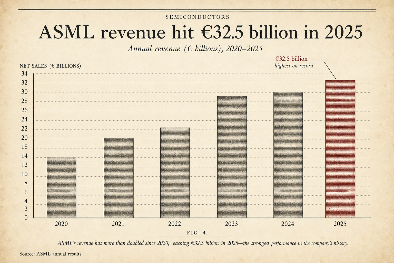
In 2025, ASML reported total net sales of €32.7 billion, gross margin of 52.8 percent, and net income of €9.6 billion. R&D investment reached €4.7 billion. The order backlog stood at €38.8 billion at year-end, equivalent to more than a full year's revenue waiting in queue. [42] [43] The company's 2026 revenue guidance of €36 billion to €40 billion, raised to as much as €43 to €45 billion in April 2026 following accelerating AI demand, positions it to nearly triple its 2020 revenue within six years. [44] Its market capitalization as of October 5, 2026 stands at approximately $714.5 billion, making it Europe's most valuable company by a wide margin, surpassing the record set by Novo Nordisk in June 2024. For context, Volkswagen and BMW have combined market capitalizations of roughly $80.5 billion. ASML is worth roughly nine times their combined value. [45] [46] [47]
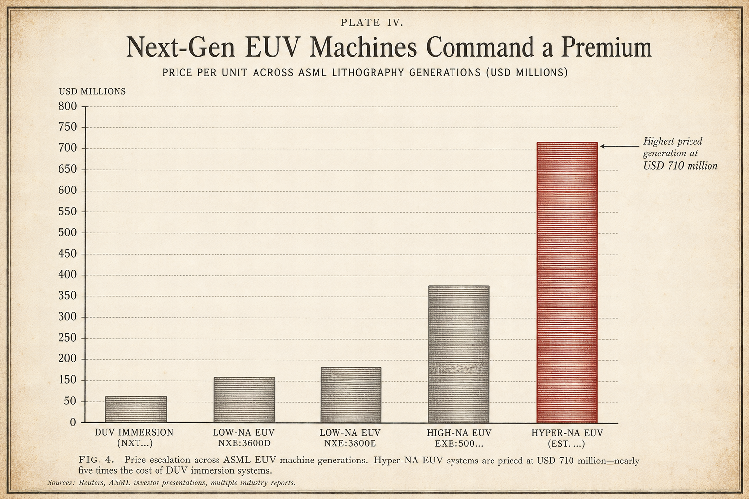
The machine price escalation is as striking as the revenue trajectory. A deep ultraviolet immersion system such as the NXT:2100i costs approximately $70 million. The current generation low-NA EUV machine, the NXE:3600D, costs approximately $150 million. Its successor, the NXE:3800E, commands approximately $180 million. The High-NA EUV systems, the EXE:5000 and EXE:5200B, are priced at $350 to $380 million per unit; Intel placed the first confirmed order for a High-NA system at "well over $340 million." An estimated future Hyper-NA system is projected to cost approximately $720 million. One analyst note observed that average EUV pricing compounded at roughly 13 percent annually over the past decade before surging another 45 percent in a single year with no orders canceled, demonstrating a degree of pricing power that would be extraordinary in any industry and is almost without precedent in capital equipment. [48] [49] [50] [51] [52]
ASML produces approximately 48 to 65 low-NA EUV systems per year, with ambitions to reach approximately 85 in 2027 and exploring production of more than 110 units in 2028. [53] [54] High-NA EUV systems are ramping from low single digits toward 10 to 20 per year by 2027 to 2028. As of September 2026, 314 EUV machines of the standard 0.33 numerical aperture variety were in operation globally, with 10 High-NA units installed and running. [55] [2] The machines' 15 to 16 week build cycle (being reduced from a recent 22 weeks) and the 12 to 18 months from order to customer-ready installation mean that ASML's current production schedule is effectively the world's production schedule for advanced semiconductor capacity. [53]
The Chain That Runs Through Everything
ASML's customers are TSMC, Samsung, Intel, SK Hynix, and Micron. But the chain of dependency extends far beyond those names.
TSMC is by industry consensus ASML's largest single EUV customer, accounting for an estimated 80 percent of EUV sales historically. TSMC's 2026 capital expenditure guidance of $52 to $56 billion, the highest in the company's history, flows substantially into lithography tools. Apple's A18 Pro chip in the iPhone 16 and its M4 processors are manufactured on TSMC's N3E process, a node that requires ASML's EUV machines. Nvidia's Blackwell AI accelerators are manufactured at TSMC using ASML's low-NA EUV systems. AMD's EPYC server chips come from the same supply chain. Tesla's Full Self-Driving processor is manufactured at TSMC. Qualcomm and MediaTek, which together supply the processing silicon for the majority of the world's smartphones, depend entirely on TSMC or Samsung for fabrication. [56] [57] [58] [59]
The AI infrastructure driving the current investment cycle sits entirely within this dependency. Every Nvidia H100 and Blackwell GPU used to train large language models, every custom accelerator Google's TPU unit designs, every AWS Trainium chip for its cloud platform: these are manufactured at TSMC or Samsung on processes that require ASML equipment. ASML CEO Christophe Fouquet has articulated the visibility of this chain publicly, noting that investors who initially focused on Nvidia's chip designs eventually understood TSMC's role, and then recognized that TSMC depends entirely on ASML for its most advanced production. [60] [61]
The dependencies run into defense and national security infrastructure as well. Advanced guidance systems, electronic warfare equipment, communications and satellite systems, and signals intelligence tools depend on the same leading-edge chips manufactured through the same TSMC-Samsung-Intel-ASML chain. There is no sovereign source of advanced semiconductor manufacturing for Western defense that bypasses ASML.
In 2025, the two largest ASML customers combined generated 38.0 percent of the company's total net sales of €32.667 billion. ASML explicitly discloses that loss of any significant customer would have "a material adverse effect" on its business. [43] The concentration of this dependency chain, from ASML to a handful of foundries to the fabless chip designers to the device makers to the cloud platforms, means that a sustained disruption at ASML would cascade through essentially every segment of the technology economy within months.
He described the US-China chip conflict as conducted "not on the basis of facts, data, and numbers, but on the basis of ideology," and warned repeatedly that locking China out of advanced semiconductor tools would accelerate rather than prevent Chinese self-sufficiency.
The Geopolitical Weapon in Plain Sight
In 2019, the Dutch government, acting under sustained pressure from Washington, refused to renew ASML's export license for its EUV machines to China. ASML had never shipped a single EUV system to a Chinese customer and has never done so since. The company states publicly that it can account for every one of the 314 EUV machines it has shipped, tracking each through remote telemetry. In June 2026, US Commerce Secretary Howard Lutnick told ASML executives that Washington believed one EUV machine had reached China in breach of the ban. ASML rejected the claim. [2] [62]
The export control regime has expanded in stages. In September 2023, the Netherlands introduced licensing requirements for advanced deep ultraviolet shipments. On January 2, 2024, the Dutch government partially revoked ASML's existing licenses for the NXT:2050i and NXT:2100i immersion systems, citing national security concerns. In September 2024, the Dutch government formally retook primary export control authority from the United States and extended restrictions to the NXT:1970i and NXT:1980i. In December 2024, the US Bureau of Industry and Security issued rules controlling node-agnostic tools and restricting software enabling advanced DUV multi-patterning configurations. [63] [64] [30]
The effect on ASML's revenue from China has been dramatic. China's share of ASML's net sales followed a striking arc: 24 percent in the second quarter of 2023, 46 percent in the third quarter of 2023 as Chinese chipmakers rushed to stockpile deep ultraviolet equipment before restrictions tightened, a peak of 49 percent in both the first and second quarters of 2024, falling to approximately 19 percent by the first quarter of 2026, and guided toward roughly 20 percent for the full year 2026. [65] [66] [67]
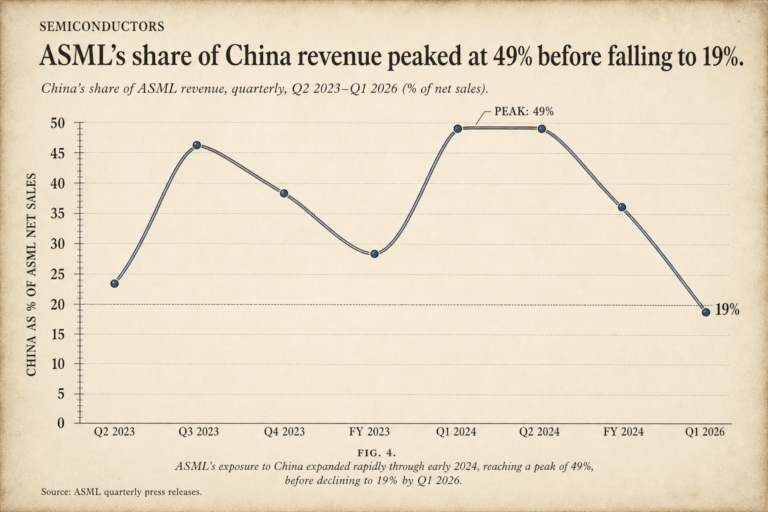
The surge was not driven by advanced tools. ASML has never sold an EUV machine to a Chinese customer. The stockpiling rush reflected Chinese chipmakers' appetite for deep ultraviolet immersion systems, which they could still legally acquire. They needed those machines to attempt what SMIC demonstrated in August 2023: using self-aligned quadruple patterning with older ASML deep ultraviolet scanners to manufacture chips at what it describes as a 7-nanometer class process. TechInsights confirmed that the Kirin 9000s chip inside Huawei's Mate 60 Pro smartphone was manufactured at SMIC using this technique. The achievement was real. The costs were also real: approximately 40 to 50 percent higher per die than TSMC's EUV equivalent, and yields of 20 to 40 percent rather than the 70 to 80 percent-plus that EUV enables. [6] [5]
The geopolitical debate around ASML contains a genuine tension that the export control regime does not resolve cleanly. Peter Wennink, who served as ASML's chief executive from 2013 to April 2024, was unusually candid about the contradiction. He described the US-China chip conflict as conducted "not on the basis of facts, data, and numbers, but on the basis of ideology," and warned repeatedly that locking China out of advanced semiconductor tools would accelerate rather than prevent Chinese self-sufficiency. "In 15 years' time they'll be able to do it all by themselves," he said, "and their market will be gone." He expected the restrictions to remain in place for "decades." [68] [69] [70] [71]
China's domestic EUV program gives some empirical weight to this concern. A working EUV prototype was reportedly completed in early 2025 inside a high-security laboratory in Shenzhen, using a laser-induced discharge plasma architecture that generates roughly 100 to 150 watts of EUV light. ASML's current systems operate at 600 watts and above. No chip has been produced using the Chinese prototype. The most optimistic Chinese government projections target production capability by 2028; analysts in the West typically estimate 2030 to 2035. [72] [73] [74] The institutional program involves thousands of researchers, with the Harbin Institute of Technology leading light source development and Changchun Institute of Optics working on optical systems. A research team led by Lin Nan, a professor at Beihang University who previously worked at ASML's research division from 2015 to 2021, published work in December 2024 reporting 3.42 percent conversion efficiency in EUV light generation from tin plasma, marginally above a 2019 benchmark of 3.2 percent established by the Amsterdam-based research consortium ARCNL. [72] China's domestic lithography company SMEE (Shanghai Micro Electronics Equipment), added to the US Entity List in December 2022, achieved mass production of 90-nanometer-capable tools in May 2025. ASML delivered machines capable of the equivalent specification to customers in 2011. [75] [76]
What Kind of Monopoly, Exactly
The word monopoly carries legal and economic meanings that do not map perfectly onto ASML's situation, and the distinctions matter.
A formal legal monopoly, the kind that attracts antitrust enforcement, typically implies control achieved through anticompetitive conduct: predatory pricing, exclusionary agreements, or regulatory capture. ASML has faced no formal antitrust investigation from the European Commission, the US Department of Justice, or any other competition authority. Its market position was built through sustained innovation, not through market manipulation. When antitrust scholars distinguish between monopolies earned through superior skill and those maintained through exclusion, ASML sits firmly in the former category. [62] [77]
A natural monopoly arises when the economics of production make a single supplier the inevitable outcome, because the capital and infrastructure requirements are so high that duplicating them is irrational. ASML fits elements of this definition too. The capital required to develop extreme ultraviolet lithography, approximately $9 to $11 billion in cumulative R&D investment by ASML alone before reaching commercial viability, spread across 30 years with no guaranteed return, is not a feasible bet for a late entrant. [78] [3] [79]
What ASML most clearly represents is a technological monopoly sustained by a bottleneck position. The company controls access to the only industrial-scale process for printing the smallest features on the most advanced chips. Without access to ASML machines, no foundry can manufacture at the process nodes that define leading-edge computing. And because leading-edge process nodes determine the performance and energy efficiency of the chips that run AI training, advanced smartphones, data center infrastructure, and defense electronics, ASML's machine is the constraint that binds all of these together.
There are legitimate counterarguments to framing this purely as monopoly power. TSMC's buying scale gives it significant leverage over ASML, and when TSMC announced in April 2026 that it would not purchase High-NA EUV machines for its A13 process node, ASML's stock fell by $16.76 billion in a single day. The customer concentration that makes ASML powerful also makes it fragile to customer decisions. By September 2026, TSMC had reversed course and committed to High-NA EUV adoption beginning in 2030, and ASML CEO Fouquet confirmed that the company's standard EUV machines were essentially fully booked through 2027. [80] [81] [82] [53] The dynamic is better described as mutual dependency than pure supplier power.
Within lithography, Canon and Nikon remain active. Canon controls approximately 8 percent of the overall lithography market and Nikon approximately 6 percent, with ASML capturing the majority in deep ultraviolet. [83] Canon's nanoimprint lithography system, the FPA-1200NZ2C, commercialized in October 2023 and first delivered to the Texas Institute for Electronics in September 2024, represents a genuine alternative for certain applications. It achieves 14-nanometer minimum linewidth at roughly a quarter of an EUV scanner's cost and one-tenth its power consumption, with throughput of at least 80 wafers per hour. For memory applications, particularly 3D NAND flash, where overlay tolerances are more forgiving, it offers real cost advantages. [84] [85] [86] [87] For leading-edge logic, its defectivity and overlay limitations (achieving roughly 3 to 10 nanometers when advanced logic requires below 2 nanometers) remain prohibitive. No foundry has committed nanoimprint to high-volume logic production. [88] [89] Nikon, meanwhile, reported its largest net loss since its 1917 founding, approximately 86 billion yen for the fiscal year ended March 2025, and is developing a new ArF immersion platform for launch in fiscal 2028, competing on price rather than capability. [90] [91]
The assessment that most accurately describes ASML is this: it holds a technological monopoly in a segment, extreme ultraviolet lithography, that has become the necessary gateway to all advanced semiconductor manufacturing. The monopoly was earned rather than captured, is uncontested in its domain, and is essentially impregnable for at least the next decade given the capital, time, knowledge, and supply chain requirements that would confront any serious challenger.
The Risks of a Single Point
What happens if something goes wrong in Veldhoven?
ASML's own 2024 Annual Report addresses this directly and without hedging. "Alternative production capacity may not be available if a major disruption were to occur," the document states, cataloguing the risks: work stoppages, fire, energy shortages, cyberattacks, flooding, pandemic, sabotage. [40] These are not hypothetical risks. On January 3, 2022, a fire in ASML's Berlin facility affected approximately 200 square meters of a 32,000-square-meter factory floor. The Berlin plant manufactures optical components including reticle chucks. The impact was limited by ASML's long lead times, which provided time to source replacement components. A larger or more sustained disruption would not afford that buffer. [92]
The geographic concentration of critical suppliers adds systemic risk. Carl Zeiss SMT operates from Oberkochen, Germany. Trumpf operates from Ditzingen, Germany. ASML's primary assembly operations are in Veldhoven. The High-NA EUV optics production, which constitutes the physical ceiling on how many High-NA machines ASML can ship per year, is concentrated in a single Zeiss facility whose manufacturing processes for the largest mirrors take approximately one year per mirror. There is no geographic redundancy in the EUV optics supply chain. [93]
The Taiwan dimension compounds these risks. TSMC accounts for approximately 54 percent of global foundry capacity and manufactures roughly 90 percent of the world's most advanced chips at nodes below 7 nanometers. Taiwan's semiconductor production vulnerability is documented in the academic literature with unusual specificity. Inventory buffers in the global chip supply chain provide approximately 90 to 120 days of resilience under steady-state demand before cascading production failures begin. TSMC's international fabs in Arizona, Japan, and Germany will collectively produce only 100,000 to 150,000 wafers per month by 2027, compared to approximately 1.4 million monthly at Taiwan facilities, meaning a Taiwan disruption would eliminate roughly 90 percent of advanced chip production capacity. [94] [95] [96]
Multiple credible sources report that ASML and TSMC have developed a capability to remotely disable EUV machines in the event of hostile takeover. TSMC Chairman Mark Liu alluded to this in a September 2022 CNN interview, suggesting any invader would find chipmaking machines non-operational. Neither ASML nor TSMC has officially confirmed the technical details of this arrangement. [94] [97]
The question of China's eventual EUV capability introduces a different category of risk: not a disruption but a structural change. If China develops production-capable EUV machinery, even at generation-lagging specifications, the export control regime that currently limits Chinese chip manufacturing becomes substantially less effective. Western intelligence estimates for this timeline range from 2032 to 2035. Chinese government projections target 2028 to 2030. The genuine uncertainty in these forecasts reflects real technical obstacles, particularly in the light source and precision optics domains, rather than political hedging. Germany has restricted Zeiss optics exports to China for EUV applications, and the specialized deposition and polishing processes that Zeiss has developed over 25 years, represented in more than 2,000 patents, are not readily reverse-engineered. [98] [72] [99]
Who Benefits, Who Pays
The concentration of semiconductor manufacturing capability in ASML's machines and TSMC's fabs generates clear winners and clear costs.
ASML shareholders have experienced returns that are difficult to characterize as anything other than extraordinary. The company's market capitalization grew from approximately $9.49 billion in November 2000 to $714.50 billion in October 2026, a compound annual growth rate of approximately 18.17 percent over 26 years. Intel's $4.1 billion equity investment in 2012 generated an estimated 17-fold return by 2023 before the company substantially reduced its position. [100] [101]
The chip design companies, Nvidia, Apple, AMD, Qualcomm, and others, benefit from access to the manufacturing capability that ASML's machines enable. AI infrastructure buildout would be physically impossible without EUV. The performance levels that make modern AI applications viable, the model sizes, the inference speeds, the energy efficiency at the chip level, are products of process nodes that require extreme ultraviolet lithography.
End users benefit in ways that are largely invisible. The smartphone in a pocket is possible because EUV lithography enabled 3-nanometer and 5-nanometer chips at commercially viable cost and power envelopes. The performance of cloud services, the capability of medical imaging AI, the precision of GPS navigation systems: all of these trace, through layers of dependency, to what ASML's machines make possible.
The costs fall on chipmakers navigating ASML's pricing power. TSMC's 2026 capex of $52 to $56 billion, the highest in its history, flows substantially toward lithography tools that only one supplier produces. The company reportedly pushed back against ASML's planned price increases for low-NA EUV machines before committing in September 2026 to the High-NA generation. [102] [74] Smaller foundries, those without the capital, the customer relationships, or the technical staff to operate advanced EUV machinery, face competitive disadvantage that compounds with each new tool generation. Academic institutions face costs for access to advanced chip fabrication ranging from $5 million for 130-nanometer processes to $725 million for 2-nanometer, with export controls and non-disclosure agreements restricting access further for students at universities in geopolitically sensitive jurisdictions. [103]
Nations without indigenous advanced semiconductor manufacturing, which is to say almost all of them, face a structural dependency on equipment, fabrication, and chip supply chains they do not control. China's experience with the export control regime illustrates the severity of this dependency, but the logic applies broadly. No European country manufactures advanced logic chips. No country outside of Taiwan, South Korea, and the United States has significant leading-edge foundry capacity. The global geography of advanced chip production is extraordinarily concentrated, and ASML's machine is the common enabler of all of it.
What Could Break the Hold
Three categories of development could eventually erode ASML's position, on timelines ranging from implausible to possible.
Genuine technological disruption would require a patterning approach that circumvents the need for EUV entirely. The most frequently cited candidates, nanoimprint lithography and directed self-assembly, address different market segments and carry different limitations. Canon's nanoimprint system demonstrates real cost advantages for memory applications but cannot meet the defect density and overlay requirements for leading-edge logic. Directed self-assembly remains at the research stage without commercial deployment on critical layers. A startup called xLight, backed by former Intel CEO Pat Gelsinger and approximately $150 million in US federal funding, is developing free-electron laser EUV sources that could challenge ASML's Cymer-supplied light source technology, but this would affect the light source subsystem rather than the scanner system itself. Substrate, another venture backed by Founders Fund, aims at X-ray lithography from particle accelerators, with planned chip factories by 2028, though the distance between a particle accelerator prototype and factory-floor semiconductor production remains enormous. [104] [73]
Chiplet architectures and three-dimensional stacking reduce the rate at which planar scaling must advance but do not eliminate it. A pure three-dimensional stacking solution at a 7-nanometer node achieves approximately 32 percent lower die cost compared to a conventional technology shrink, buying meaningful time. However, the logic dies at the heart of stacked systems still require leading-edge process nodes. Memory continues to demand EUV-enabled shrinks. Thermal and power density constraints limit how aggressively chips can be stacked. [105] [106] The semiconductor industry has consistently found that advanced packaging complements rather than replaces lithographic scaling.
Chinese domestic capability remains the wild card with the widest confidence interval. If SMEE or a successor entity achieves production-capable EUV by 2030, and particularly if it achieves it at sub-$200 million price points by accepting lower throughput in exchange for domestic supply, the export control regime would face a fundamental challenge. The investment is real: China has committed approximately €37 billion to domestic EUV development. [107] The obstacles are also real: the precision optics, the light source engineering, the vacuum systems, and the control software represent decades of accumulated institutional knowledge that cannot be purchased from a catalog.
The most honest assessment of ASML's durability is this. Through 2030, the monopoly is structurally unassailable. The company's 2030 revenue scenario, modeled at the 2024 Investor Day, projects €44 billion to €60 billion with gross margins of 56 to 60 percent, implying continued pricing power and demand growth. [108] [58] Beyond 2030, the emergence of Chinese domestic capability, the maturation of alternative patterning approaches, or some unforeseen technological discontinuity could reshape the landscape. None of these scenarios represents an imminent threat. The more pressing question for the immediate future is not whether ASML's monopoly persists but whether ASML can build machines fast enough to supply the demand created by the AI infrastructure buildout, while navigating the geopolitical pressures that have simultaneously made it the world's most important manufacturer and one of the most contested instruments of great-power competition.
The company began in a leaky shed adjacent to Philips buildings in Eindhoven, nearly died twice before it shipped a meaningful product, spent 30 years and billions of dollars on a machine no one was certain could be made to work commercially, and ended up the indispensable enabler of the most consequential technological buildout of the current era. That it sits at the center of everything, and that almost no one outside the industry knows its name, is perhaps the most revealing fact about how modern technological infrastructure actually works.
- ASML manufactures only about 15 percent of its EUV machines' components internally.
- The AI infrastructure driving the current investment cycle sits entirely within this dependency.
- The assessment that most accurately describes ASML is this: it holds a technological monopoly in a segment, extreme ultraviolet lithography, that has become the necessary gateway to all advanced semiconductor manufacturing.
- Through 2030, the monopoly is structurally unassailable.
Get the next issue in your inbox.
Free, weekly. One company or market, taken completely apart — every figure sourced and verified with Valyu DeepResearch.
Issue queued.
Your next cited briefing is on its way to .